-
Your shopping cart is empty!

Precision Machining for Semiconductor Equipment: Meeting the Sub-Micron Challenge with WENZEL CMM Solutions
Friday July 17th, 2026
-
0 lượt xem
The Semiconductor Industry – The Foundation of the Digital Era
The semiconductor industry has become one of the primary drivers of the global digital economy. From smartphones and electric vehicles to medical devices, artificial intelligence (AI), cloud computing, and hyperscale data centers, virtually every modern technology relies on increasingly powerful semiconductor chips.
Producing these advanced integrated circuits requires highly sophisticated equipment, including photolithography systems, wafer handling equipment, vacuum chambers, process modules, and robotic automation systems, all operating with near-perfect precision. Consequently, the mechanical components used in semiconductor manufacturing equipment must be machined to tolerances measured in micrometers (μm) and, in many cases, nanometers (nm).
This is why precision machining for semiconductor equipment is considered one of the most demanding disciplines in modern manufacturing.
Why Does the Semiconductor Industry Require Sub-Micron Precision?
In many manufacturing industries, a tolerance of ±0.01 mm is considered highly accurate. However, for semiconductor equipment, this level of precision is far from sufficient.
A dimensional deviation of only a few micrometers can result in:
- Wafer positioning errors
- Motion system misalignment
- Reduced photolithography accuracy
- Lower production yield
- Multi-million-dollar manufacturing losses
Therefore, semiconductor manufacturers require not only exceptional machining accuracy but also long-term dimensional stability throughout the component’s operational life.
Challenges in Precision Machining for Semiconductor Equipment
1. Extremely Tight Tolerances and Complex Geometries
Critical semiconductor components such as:
- Wafer Chucks
- End Effectors
- Vacuum Plates
- Precision Brackets
- Robotic Arms
often feature thin-wall structures combined with relatively large overall dimensions.
During CNC machining, residual stress develops within the material. Once the component is released from the fixture, spring-back may occur, causing dimensional changes of only a few micrometers—yet enough to exceed the specified tolerance.
For modern photolithography systems, these seemingly insignificant dimensional deviations can directly impact wafer positioning accuracy.
2. Surface Finish and Contamination Control
Unlike conventional precision machining, semiconductor components require not only exceptional surface finish but also absolute cleanliness.
Residual contaminants such as:
- Cutting fluids
- Metallic particles
- Ultra-fine dust
- Chemical residues
can migrate into cleanroom environments and compromise semiconductor manufacturing processes.
As a result, surface roughness requirements must always be accompanied by stringent contamination controlprotocols.
3. Thermal Stability
Semiconductor manufacturing equipment operates in tightly controlled thermal environments.
If machining-induced stresses are not completely relieved, thermal expansion may alter:
- Assembly positions
- Mechanical clearances
- Parallelism
- Perpendicularity
Even dimensional changes of only a few micrometers can significantly reduce equipment accuracy.
4. Complete Traceability
Semiconductor manufacturers demand comprehensive quality documentation, including:
- Material certificates
- Machining process records
- Calibration certificates
- Dimensional inspection reports
- Quality control documentation
Complete traceability is essential for ensuring compliance throughout the semiconductor supply chain.
Advanced Machining Solutions for Semiconductor Components
Multi-Stage CNC Machining to Minimize Residual Stress
Rather than removing material in a single heavy machining operation, semiconductor components typically undergo multiple manufacturing stages:
- Rough machining
- Semi-finish machining
- Stress-relief heat treatment
- Finish machining
- Ultra-finish machining
This process minimizes distortion while ensuring long-term dimensional stability.
Ultrasonic Cleaning
Following machining, components undergo Ultrasonic Cleaning to remove:
- Cutting oils
- Metallic debris
- Abrasive particles
- Chemical residues
The components are subsequently dried using clean air before being double-bagged inside a certified cleanroom environment to prevent contamination during transportation.
Controlled Manufacturing Environment
Many semiconductor component manufacturers operate dedicated production areas with controlled:
- Temperature
- Humidity
- Airborne particles
- Mechanical vibration
Maintaining a stable manufacturing environment significantly improves machining consistency and measurement accuracy.
Precision Measurement – The Key to Quality Assurance
Precision machining represents only one aspect of semiconductor manufacturing.
Equally important is the ability to verify that precision.
Conventional measuring tools such as calipers and micrometers cannot reliably inspect components requiring sub-micron tolerances.
Instead, manufacturers rely on Coordinate Measuring Machines (CMMs) to evaluate:
- Geometric dimensions
- Flatness
- Perpendicularity
- Concentricity
- Surface profiles
- Complex contours
- GD&T (Geometric Dimensioning and Tolerancing)
The Role of WENZEL Coordinate Measuring Machines in the Semiconductor Industry
With more than 50 years of experience, WENZEL is recognized as one of the world’s leading manufacturers of Coordinate Measuring Machines (CMMs), serving industries with the highest precision requirements, including aerospace, automotive, mold & die, and semiconductor manufacturing.
WENZEL CMM systems are specifically engineered to deliver exceptional measurement accuracy through:
- Natural granite machine structures providing superior thermal stability and vibration damping
- Air-bearing guideways for smooth, frictionless motion
- Compatibility with both touch-trigger probes and high-speed scanning probes
- Comprehensive GD&T inspection capabilities
- Advanced measurement software supporting automation, digital reporting, and Industry 4.0 integration
Thanks to their outstanding repeatability and long-term measurement stability, WENZEL CMMs enable manufacturers to identify dimensional deviations early in the production process, reducing scrap rates and improving quality assurance throughout semiconductor component manufacturing.
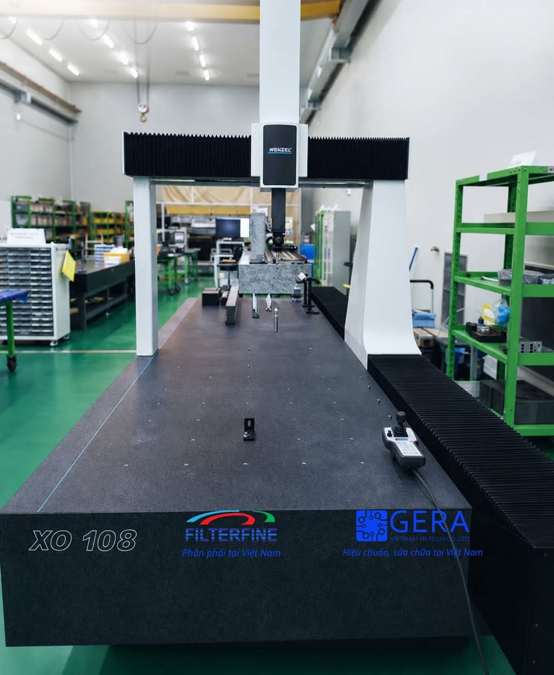
Filterfine Vietnam – Your Trusted WENZEL CMM Solution Provider
As an industrial metrology solution provider in Vietnam, Filterfine Vietnam supplies WENZEL Coordinate Measuring Machines (CMMs) together with comprehensive engineering support.
Our services include:
- CMM selection and application consulting
- System installation and commissioning
- Measurement programming and operator training
- Preventive maintenance and calibration support
- Development of inspection procedures compliant with international standards
- Integration of CMM systems into Quality Management Systems (QMS) and Smart Manufacturing environments
These complete metrology solutions help manufacturers in precision engineering, electronics, and semiconductor industries improve quality control, reduce manufacturing defects, and meet increasingly stringent global supply chain requirements.
Achieving the Zero Defect Philosophy
In semiconductor manufacturing, “good enough” is never good enough.
The industry’s ultimate objective is Zero Defect Manufacturing, ensuring that no defective component advances to the next production stage.
Achieving this objective requires the integration of:
- Multi-axis precision CNC machining
- In-Process Probing
- 100% CMM inspection for critical components
- Digital measurement data management
- Complete material and process traceability
- Strict environmental and cleanroom control
The combination of advanced manufacturing technologies and high-precision metrology forms the foundation for meeting the increasingly demanding requirements of today’s semiconductor industry.
Conclusion
Precision machining for semiconductor equipment requires much more than advanced CNC technology. It demands carefully controlled machining processes, residual stress management, clean manufacturing environments, and highly accurate metrology systems capable of verifying sub-micron tolerances.
As semiconductor technology continues to evolve, investing in advanced inspection solutions such as WENZEL Coordinate Measuring Machines (CMMs) enables manufacturers to improve dimensional accuracy, reduce defects, optimize production yield, and comply with the world’s most demanding quality standards.
With extensive experience in industrial metrology, Filterfine Vietnam provides WENZEL CMM solutions, application consulting, installation, training, calibration, and technical support, helping manufacturers build highly accurate, stable, and data-driven production processes while advancing toward the ultimate goal of Zero Defect Manufacturing.
Tin liên quan
- WENZEL CMM: A Solution for Every Inspection Need
- WENZEL XP: High-Accuracy Coordinate Measuring Machine for the Shop Floor
- Kalrez® vs. Viton™: Which Sealing Material Is Right for Your Application?
- Three Layers of Data Continuity with the Lighthouse ApexZ Particle Counter
- Industrial Wastewater Monitoring: Inline Concentration Measurement for Better Process Control